
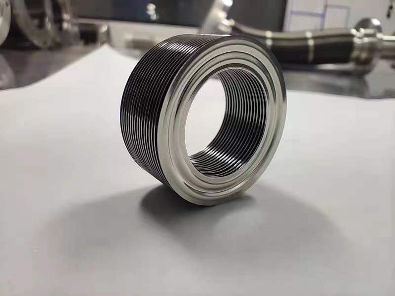
On August 4, 2026, Kioxia and SanDisk unveiled their ninth-generation 3D flash memory technology, claiming the industry’s highest bit density for QLC NAND. Three weeks later, the pair announced plans for a $31 billion third fab at Kioxia’s Iwate Prefecture site in Japan — a direct bet that AI data-center demand for NAND will keep climbing. The NAND market, valued at roughly $77 billion in 2026, is projected to reach $199 billion by 2035 at an 11% CAGR, according to Business Research Insights. Samsung’s FMS 2026 keynote laid out a similar next-generation 3D-memory vision.
For vacuum engineers, the number behind the headlines is the layer count. Every generation of 3D NAND adds layers, and every layer adds process steps — and the process steps that define 3D NAND are vacuum steps. This is the same logic we applied to 3D DRAM architecture, now at industrial scale in flash.
Why 3D NAND Is a Stack, Not a Chip
Planar NAND scaled by shrinking; 3D NAND scales by stacking memory cells vertically. A 400-layer device is, physically, a multi-kilometer stack of alternating oxide/nitride films on a single wafer, drilled through by hundreds of millions of vertical channels. The build sequence is a repeating loop of two vacuum processes:
- Deposition — alternating SiO₂ and SiN layers deposit in vacuum CVD/PECVD reactors, each pair of layers being one potential cell row.
- Etch — the vertical channel holes and word-line trenches are plasma-etched through the entire stack — aspect ratios of 100:1 and climbing, in high-density plasma etch tools.
Then come the fill steps — the channel polysilicon, the high-k dielectrics and metal word lines — again deposited in vacuum. Multiply by 400+ layers and a 3D NAND wafer can pass through more than a hundred vacuum processing steps, each in its own chamber, each with its own pumps, valves, feedthroughs and bellows.
The Vacuum Hardware Every Layer Stack Depends On
Cluster tool architecture
Memory makers build 3D NAND in cluster tools: a central vacuum transfer module moves wafers between process chambers through slit valves — literally hundreds per tool. The bellows that seal each slit valve cycle hundreds of thousands of times a year; we analyzed the economics of these seals in slit valve hardware.
Deposition chamber hardware
CVD/PECVD chambers run at elevated temperatures with corrosive precursors. Heater power and thermocouple feedback cross the wall through vacuum feedthroughs; gas lines are valved and flexed with edge welded bellows; chamber lids lift and pedestals move through bellows-sealed actuators. Our high temperature feedthrough guide covers the thermal side of that specification.
Etch tool vibration control
High-density plasma etchers generate strong vibration and thermal cycling. Pump isolation bellows and bellows-designed flexible connections protect process uniformity — the same requirements we documented for metrology and inspection tools.
Leak integrity at scale
With hundreds of chambers per fab, leak-test throughput is a production metric. Bellows, valves and assemblies that ship pre-leak-tested to 1×10⁻⁹ mbar·L/s, per our leak testing standards, cut bring-up time that costs more per hour than the components cost per unit.
Why the $31B Fab Is a Vacuum Market Signal
Kioxia and SanDisk’s third Iwate fab is a response to the AI storage supercycle — and a procurement program for every vacuum component a memory fab consumes: thousands of pumps, tens of thousands of valves, and a permanent replacement stream of bellows and seals. The same signal is coming from Samsung’s FMS 2026 roadmap and from Chinese memory makers scaling their own 3D NAND. Each new fab is a new, long-duration demand center for vacuum hardware — exactly the pattern we traced for the broader vacuum equipment market.
Component Selection Priorities for NAND Fabs
- Cycle life — slit valve and isolation valve bellows must deliver millions of cycles; demand documented fatigue life.
- Particle control — metal bellows seals beat elastomers in clean processes.
- Process compatibility — fluorinated chemistry and high temperatures drive material selection (316L, AM350, Inconel) per our materials comparison.
- Series reliability — memory fabs run identical tools in fleets; component-to-component repeatability is a qualification gate.
The Alpha Technology Angle
Alpha Technology manufactures custom edge welded bellows, bellows-sealed valve assemblies, vacuum feedthroughs and vacuum gaskets for memory and logic fabs — helium-leak-tested, serialized and cycle-documented. Deposition and etch tool OEMs and memory fab spares teams can contact our engineering team for qualified hardware.
FAQ
How many layers does 3D NAND have?
Current ninth-generation products exceed 400 layers; every generation adds layers, each requiring repeated vacuum deposition and etch steps.
Why is 3D NAND manufacturing vacuum-intensive?
The alternating oxide/nitride stack is built by vacuum CVD, the vertical channels and trenches are plasma-etched in vacuum, and fills and metallization deposit in vacuum — over 100 vacuum steps per wafer.
What did Kioxia and SanDisk announce in 2026?
In August 2026 they unveiled ninth-generation 3D flash with the industry’s highest QLC bit density, and announced a $31 billion third fab in Iwate Prefecture, Japan.
How big is the NAND flash market?
Business Research Insights values the NAND flash market at $77 billion in 2026, projected to reach $199 billion by 2035 at an 11% CAGR.
Supporting NAND fab capacity growth? Contact Alpha Technology for cycle-rated bellows, valves and feedthroughs.