
In February 2026, researchers reported that all-vacuum-deposited (solvent-free) perovskite solar cells — including perovskite-on-silicon tandems — had moved a decisive step closer to scalable manufacturing, and a companion study in Nature Materials demonstrated crystal-facet-directed control over vacuum-deposited perovskite films. The appeal is straightforward: perovskite solar cells are cheap, efficient, and — when made by vacuum deposition — free of the solvents that have held back industrial production and recycling.
Perovskites are the most exciting story in photovoltaics since silicon itself, and their manufacturing future is a vacuum equipment story.
Why Vacuum Deposition Wins for Perovskites
1. Precision without solvents
Solution-based perovskite processing is fast but suffers from batch-to-batch variation, solvent toxicity and pinholes. Vacuum deposition (thermal evaporation and sputtering) gives atom-level thickness control and produces uniform films across large areas — the same reason the display and semiconductor industries use vacuum coating everywhere.
2. Tandem compatibility
Perovskite-on-silicon tandem cells stack a perovskite top cell on a silicon bottom cell to beat the silicon efficiency limit (33%+ laboratory, ~30% commercial roadmap). Depositing the perovskite layer on a textured silicon cell requires conformal, solvent-free coating — vacuum deposition is the only mature route.
3. Scale-up economics
Vacuum deposition equipment is proven at gigawatt scale from the thin-film PV and display industries. For perovskite manufacturers, that means the toolchain — evaporators, sputterers, and their vacuum subsystems — exists today.
4. The efficiency numbers driving the push
Perovskite-silicon tandems have now surpassed 34% efficiency in laboratory cells, and commercial modules are expected to enter the 30% class during this decade — versus roughly 22-24% for mass-produced silicon modules. At utility scale, those efficiency points translate into billions of dollars of levelized energy cost savings, which is why major cell manufacturers and equipment builders are investing in vacuum deposition capability now. For the vacuum industry, the interesting number is not the efficiency record but the tool count: each gigawatt of tandem capacity requires multiple evaporators, sputterers and ALD reactors, each consuming the same feedthroughs, bellows and valves that silicon fabs consume.
The Vacuum Toolchain for Perovskite Fabs
- Thermal evaporators: organic and inorganic perovskite precursors are evaporated from heated sources in vacuum; shutters, thickness monitors and substrate stages are all bellows-sealed mechanisms.
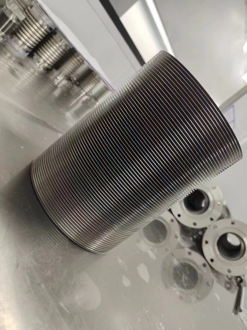
- Sputterers for electrodes: transparent conductive oxides (ITO, and indium-free alternatives) are sputtered in vacuum; target shutters and shields use edge welded bellows for sealed motion.
- Atomic layer deposition (ALD): interface and encapsulation layers use ALD for pinhole-free films — a fully vacuum process with precision feedthroughs and gas systems.
- Encapsulation: perovskite modules must be hermetically sealed against moisture and oxygen; glass-to-glass sealing and edge sealing run in vacuum or controlled atmosphere, with the same sealing hardware used in optoelectronics hermetic packaging.
What Perovskite Equipment Builders Need From Vacuum Suppliers
Perovskite production tools are cost-sensitive — the entire point is cheaper solar — which changes component priorities:
- Reliability over absolute precision: evaporation chambers run continuously; bellows and valves must survive millions of cycles without maintenance.
- Uniformity at scale: a 2.4m-wide substrate needs long-stroke, low-spring-rate bellows for shutters and mask handling — design work covered in the design guide.
- Clean, low-outgassing materials: perovskite films are sensitive to contamination; 316L and specialty alloys keep the vacuum clean. The material guide explains the choices.
- Cost per cycle: for solar-scale production, component lifetime per dollar is a specification — fatigue engineering matters.
The Opportunity for Vacuum Component Makers
Perovskite capacity is expanding from pilot lines to early gigawatt fabs in 2026-2028, notably in China, Europe and the US. Each gigawatt of capacity needs evaporators, sputterers and ALD tools — and each tool needs hundreds of vacuum components. For manufacturers of edge welded bellows, vacuum feedthroughs and chambers, thin-film PV is a fresh market that is less cyclical than semiconductors and growing from a small base.
Alpha Technology for Thin-Film and Solar Tooling
Alpha Technology builds custom edge welded bellows, vacuum feedthroughs and formed bellows for evaporation, sputtering and ALD systems serving thin-film PV, displays and batteries — leak tested, cleanroom assembled and documented. Contact our engineering team with your substrate size and duty cycle.
FAQ
Why are perovskite solar cells important?
Perovskites combine high efficiency with low-cost manufacturing; tandem perovskite-on-silicon cells can exceed the efficiency limit of silicon alone.
What is all-vacuum deposition for perovskites?
Growing perovskite films by thermal evaporation and sputtering in vacuum instead of coating from solvents — giving precise, uniform, solvent-free films suited to mass production.
Which vacuum processes do perovskite fabs use?
Thermal evaporation, sputtering (electrodes), ALD (interfaces/encapsulation) and hermetic module sealing — all vacuum or controlled-atmosphere processes.
Can existing vacuum component technology serve perovskite tools?
Yes — the toolchain is mature; what matters is cost-effective reliability at solar-scale duty cycles, which Alpha Technology engineers for.
Designing deposition or encapsulation tooling? Contact Alpha Technology for vacuum components sized to your substrate and production schedule.