
Yole Group’s 2026 Power SiC — Markets and Applications report projects the power silicon carbide market past $11 billion within five years, driven by EVs and, increasingly, AI data-center power. The growth is being built on a hard engineering transition: the industry is ramping from 150mm (6-inch) to 200mm (8-inch) SiC wafers, cutting cost per chip by roughly a third and multiplying fab throughput.
In parallel, capacity announcements are landing weekly: Mitsubishi Electric completed its new 8-inch SiC fab in Kikuchi, Japan, GlobalWafers is converting part of its Sherman, Texas epitaxy plant to SiC, and multiple Chinese and European players are adding 200mm lines. Beneath the wafer-size headlines sits a quieter fact: nearly every step of SiC device fabrication happens in vacuum.
Why SiC Manufacturing Is Vacuum-Intensive
1. Epitaxy: the crystal grows in vacuum
SiC devices are built on epitaxial layers grown by chemical vapor deposition (CVD) at 1,500-1,700 °C in a vacuum/low-pressure chamber. The epi layer’s quality — doping uniformity, defect density — determines the device’s blocking voltage. Epi tools are large, hot vacuum chambers whose every seal, feedthrough and gas line must hold integrity at extreme temperature. A single micro-leak ruins a run worth hundreds of wafers.
2. Implantation and high-temperature anneal
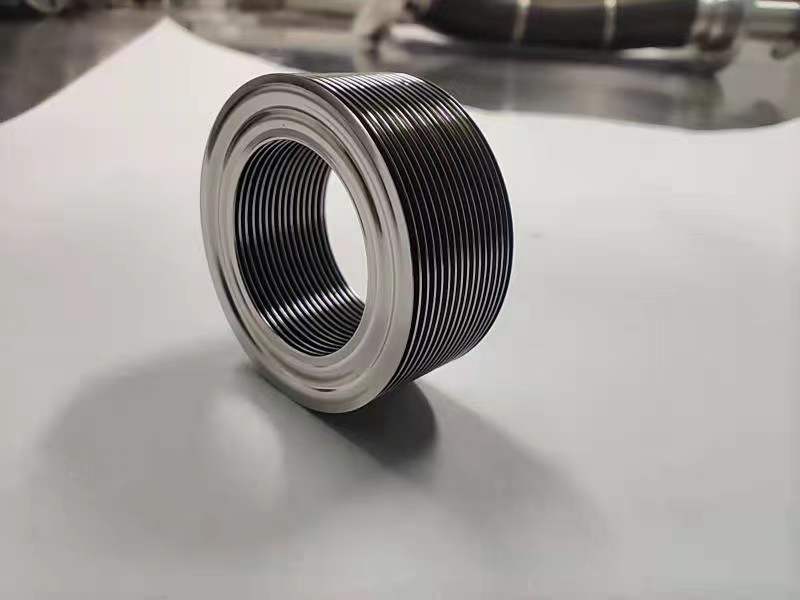
Dopants are introduced by ion implantation (a vacuum process) and activated by annealing at 1,600-1,800 °C — the hottest step in any semiconductor process. Anneal furnaces are vacuum systems where edge welded bellows and metal seals must survive repeated thermal cycling between room temperature and 1,800 °C without leaking. The materials and fatigue rules for this duty are in our material guide and design guide.
3. Sputtering, etching and passivation
Ohmic contacts are sputtered in vacuum, device structures are etched in plasma (RIE) chambers, and passivation layers are deposited by CVD. All are vacuum processes with load locks, bellows-sealed stages and RF feedthroughs — the same architecture as silicon fabs, covered in our article on edge welded bellows for semiconductor applications.
4. Trench processes and edge termination
Modern SiC MOSFETs and diodes are vertical devices: the current flows through the wafer, and the voltage-blocking structure (the edge termination, typically a junction termination extension) is formed by implanted regions and etched trenches. Trench etching in SiC is a plasma process, and the implant/anneal sequence that forms the termination is vacuum-based. These steps add several vacuum chambers per wafer, and because SiC wafers cost several times more than silicon, a single chamber leak that ruins a batch is an expensive event. This is why SiC fabs buy vacuum feedthroughs and edge welded bellows with the same documentation discipline as leading-edge logic fabs.
What the 200mm Transition Changes
Moving from 150mm to 200mm is not a simple scale-up. It changes the vacuum hardware in four concrete ways:
- Bigger chambers, longer strokes: a 200mm wafer is 78% larger in area; stages travel farther and chambers are bigger. Long-travel edge welded bellows with low spring rates become the norm.
- Higher throughput expectations: 8-inch lines are designed for volume; bellows and valves must hit semiconductor-grade cycle life, not R&D-grade.
- More vacuum steps per wafer: SiC devices are vertical (trench MOSFETs, diodes) — the trench etch and fill steps add vacuum process steps per wafer.
- Automation and 24/7 operation: production fabs run continuous; load locks, slit valves and transfer robots cycle millions of times, which is where component quality is really tested.
The Supply Chain Squeeze
SiC equipment is still a relatively small market, so the vacuum component supply base serving it is small too. As 8-inch lines multiply, the demand for high-temperature bellows, cryo-pumping support and clean, leak-tested hardware is growing faster than the qualified supplier base. This mirrors the situation in logic fabs we analyzed in the $403 billion semiconductor quarter — early qualifiers win capacity.
Alpha Technology for SiC and Wide-Bandgap Fabs
Alpha Technology supplies custom edge welded bellows, vacuum feedthroughs and formed bellows for SiC epitaxy, anneal, sputter and etch tools — high-temperature alloys like AM350 and Inconel, 100% helium leak tested with serialized reports, cleanroom assembled. We support full qualification packages for new 200mm lines. Contact our engineering team with your process temperature and envelope.
FAQ
Why is SiC important for power electronics?
Silicon carbide devices switch faster and handle higher voltages and temperatures than silicon, cutting losses in EVs, solar inverters, grid equipment and AI data-center power.
Why is the transition to 200mm SiC wafers significant?
200mm wafers roughly halve cost per die versus 150mm and enable high-volume manufacturing, which the market needs to reach $11B+ in five years.
Which SiC process steps use vacuum?
Epitaxy (CVD), ion implantation, high-temperature anneal, sputtering, plasma etching and passivation deposition — essentially the entire device fabrication flow.
How do I qualify vacuum components for SiC tooling?
Demand high-temperature alloy selection, 100% leak testing, cleanroom assembly and cycle-life data; Alpha Technology provides all four with every shipment.
Building or qualifying SiC process tooling? Contact Alpha Technology — send your process conditions and envelope for a vacuum component design.