
In mid-August 2026, TrendForce reported that Samsung Electronics had lifted its HBM4 production yield to around 80%, intensifying the race with SK Hynix for sixth-generation high-bandwidth memory. Industry watchers have long flagged 2027 as the year hybrid bonding machines become critical, as memory makers move toward mass production of 20-layer HBM4 stacks. Behind the yield headlines sits a quiet engineering fact: hybrid bonding — the technology that lets memory chips stack without solder bumps — is a vacuum process from start to finish.
HBM4 is the highest-volume commercial deployment of hybrid bonding to date, and its ramp is a vacuum equipment story.
What Hybrid Bonding Actually Is
Hybrid bonding joins two wafers or dies by copper-to-copper and dielectric-to-dielectric contact at room temperature, with no solder, no flux and no underfill gap. The contact surfaces must be atomically flat and clean: a single particle or a few nanometers of surface roughness means a non-contact, a void, or a bond that fails after thermal cycling. That is why the process chamber is a clean vacuum environment — and why every step in the flow is engineered like a lithography process, not like an assembly step.
The Vacuum Steps Inside a Hybrid Bonder
1. Plasma activation
Before contact, the copper pads and dielectric surfaces are activated in a plasma chamber — typically Ar/N2 or forming-gas plasma under vacuum — to remove native oxide and hydroxylate the surfaces. The activation step sets the surface energy that drives the initial room-temperature bond. Chamber cleanliness, gas purity and process repeatability are everything; this is a vacuum feedthrough and precision gas-system environment.
2. Alignment and room-temperature bonding
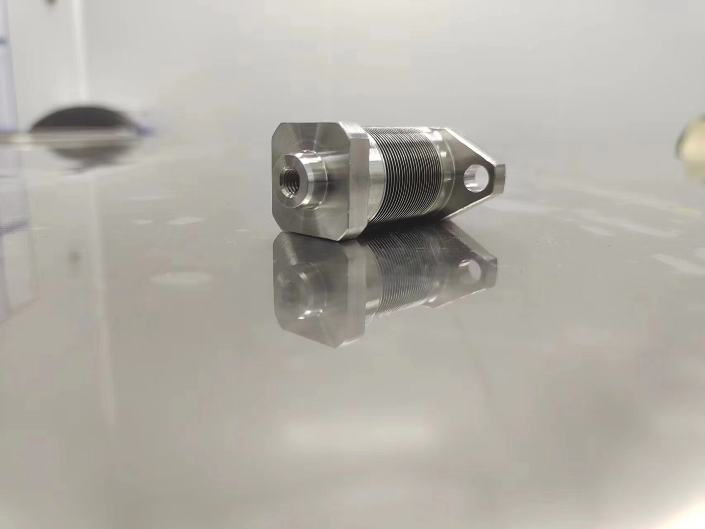
Aligned die-to-wafer or wafer-to-wafer contact happens in a controlled atmosphere or vacuum bond chamber with sub-micron alignment. The bonding head presses with precise force while edge welded bellows seal the actuation and absorb the mechanical motion — the same bellows-sealed stage technology used across semiconductor tooling, covered in our design guide.
3. Anneal
The room-temperature bond is strengthened by annealing at 150-350 °C, where copper diffuses across the interface and grain growth welds the pads. Anneal furnaces are vacuum or controlled-atmosphere systems; the thermal budget and uniformity directly determine yield. As HBM4 stacks grow toward 20 layers, each layer adds an activation-bond-anneal cycle — multiplying the vacuum process steps per package by the number of tiers.
Why 20 Layers Multiply the Challenge
HBM4 stacks 16 or more DRAM dies; roadmaps point to 20+ layers with hybrid bonding replacing the TC-NCF (thermal-compression with non-conductive film) process used in HBM3E. Every additional layer means: more bond interfaces to keep defect-free, more cumulative warpage to manage during bonding, and more wafer starts for the memory makers who must roughly 8x their 1c DRAM production, as SK Hynix has signaled. The tool set — plasma activation, bonders, anneal furnaces — grows one-for-one with layer count, and each tool consumes the same vacuum component inventory we describe for advanced packaging plants and panel-level packaging lines.
The Vacuum Component Load of a Hybrid Bonding Fab
- Load locks and transfer robots: wafers enter and leave process chambers through vacuum load locks with bellows-sealed slit valves.
- Plasma chambers: RF power crosses the wall through RF feedthroughs; electrodes and shutters use edge welded bellows.
- Precision stages: alignment stages and bond heads need low-friction, low-outgassing bellows with millions of cycle life.
- Gas and vacuum integrity: 100% helium leak testing on every chamber, the framework in our leak testing guide.
Cleanliness Is the Yield Driver
Hybrid bonding is unforgiving of contamination: a particle on a bond pad is a dead interconnect, and a water molecule on the surface ruins the activation. That is why bonding fabs treat edge welded bellows, feedthroughs and chambers as cleanroom components — vacuum-fired, cleanroom-assembled, with material certification for low outgassing. The material guide covers the alloy choices; the cleanliness discipline is the same one we detail for hermetic optoelectronics packaging.
Alpha Technology for Hybrid Bonding and Advanced Packaging
Alpha Technology supplies custom edge welded bellows, vacuum feedthroughs and bellows-sealed components for plasma activation, bonding and anneal tools serving HBM, logic-on-logic and chiplet packaging — semiconductor-grade cleanliness, helium leak tested, with cycle-life and outgassing documentation. Contact our engineering team with your process envelope.
FAQ
What is hybrid bonding?
Hybrid bonding joins dies or wafers by direct copper-to-copper and dielectric-to-dielectric contact at room temperature, without solder bumps, then strengthens the bond by annealing.
Why is hybrid bonding important for HBM4?
HBM4 stacks more DRAM layers at finer pitch than HBM3E; hybrid bonding provides the interconnect density and reliability needed for 16-20+ layer stacks.
Why is vacuum required for hybrid bonding?
Surface activation (plasma), particle-free contact and uniform annealing all require controlled vacuum or clean atmosphere; contamination of the bond interface directly reduces yield.
What vacuum components does a hybrid bonder contain?
Load locks, plasma chambers, precision bellows-sealed stages, RF and instrumentation feedthroughs, and anneal furnaces — all qualified by helium leak testing.
Building bonding or activation tooling? Contact Alpha Technology for vacuum components qualified to semiconductor cleanliness standards.