
On May 29, 2026, the world’s first diamond semiconductor factory was completed in the town of Okuma, Fukushima Prefecture, Japan — the same region rebuilding around the Fukushima Daiichi nuclear site. Diamond is the ultimate wide-bandgap semiconductor: five times the breakdown field of silicon carbide, the highest thermal conductivity of any material, and radiation hardness that makes it a candidate for power electronics, 5G/6G RF, and quantum sensing. Japanese industry groups and government programs have spent over a decade preparing this moment.
Diamond semiconductors are headline news for their physics. For vacuum engineers, they are interesting for a different reason: diamond device fabrication is almost entirely a vacuum process story.
Why Diamond Fabs Are Vacuum Factories
1. Growth: MPCVD in vacuum
Device-grade diamond is grown by microwave plasma chemical vapor deposition (MPCVD) — a methane/hydrogen plasma is struck inside a vacuum chamber and diamond nucleates and grows layer by layer on a substrate. The plasma must be exceptionally uniform, which means the chamber pressure (typically 50-200 mbar) and gas flow must be controlled precisely, and the chamber’s vacuum integrity defines film purity. A leaking chamber introduces oxygen, which poisons diamond growth.
2. Doping: ion implantation and annealing
Diamond’s extreme bonding makes diffusion doping impossible; dopants are added by ion implantation followed by high-temperature annealing (up to 1,700 °C) — both vacuum processes. Implanters and anneal furnaces are sealed systems with vacuum feedthroughs for power, gas and sensing, and any leak at anneal temperature is fatal to device yield.
3. Etching and surface termination
Device structures are etched in oxygen-based plasma (RIE) and surfaces are hydrogen- or oxygen-terminated in controlled environments. These steps run in vacuum chambers with bellows-sealed stages and load locks — the same architecture as silicon fabs, just with different chemistry. Our article on edge welded bellows for semiconductor applications describes why load-lock reliability matters at these scales.
4. Packaging and hermetic sealing
Power diamond devices — Schottky diodes, FETs — must be packaged hermetically to protect the terminated surfaces and handle the extreme power densities. Hermetic packaging is a vacuum/controlled-atmosphere process: the sealing and testing disciplines are the same as the vacuum hardware we describe in sealing hardware for photonics packaging.
What Diamond Manufacturing Demands From Vacuum Components
- High-temperature integrity: anneal furnaces run to 1,700 °C; components must survive extreme thermal cycling without leaking.
- Plasma compatibility: MPCVD and RIE chambers expose hardware to hydrogen and oxygen plasmas; materials like 316L, Inconel and specialty alloys are required — the material guide compares them.
- Cleanliness: diamond growth is sensitive to contaminants at the parts-per-billion level; chambers and components must be cleanroom-grade.
- Long cycle life: a production diamond line runs 24/7; bellows in load locks and stages must survive millions of cycles. The design guide explains the fatigue engineering.
5. Diamond for quantum and sensing
Beyond power devices, diamond hosts color-center qubits — nitrogen-vacancy (NV) centers — that are among the most promising platforms for quantum sensing and quantum networks. NV-center diamond devices are fabricated with the same vacuum process family: MPCVD growth, implantation, and surface termination in controlled environments. That means the diamond semiconductor fab in Okuma is not only a power-electronics factory; it is a seed facility for the quantum supply chain, which multiplies the vacuum hardware demand further. The vacuum requirements for quantum-grade diamond overlap with the cryostat hardware we discuss in UHV components inside a dilution refrigerator.
A New Supply Chain, Built on Familiar Hardware
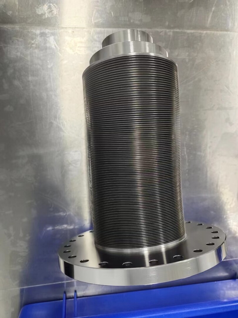
The diamond semiconductor supply chain is young, but its tools are built by the same vacuum equipment industry that serves silicon and SiC. MPCVD systems, implanters, annealers and etchers all need edge welded bellows, feedthroughs, valves and chambers — and they need suppliers who can deliver qualified, leak-tested hardware quickly. For component manufacturers, wide-bandgap fabs (diamond, SiC, GaN) represent the fastest-growing segment of the vacuum hardware market outside AI logic.
Alpha Technology for Wide-Bandgap Fabs
Alpha Technology manufactures custom edge welded bellows, vacuum feedthroughs and formed bellows for silicon, SiC and diamond fab equipment — high-temperature alloys, 100% helium leak testing, cleanroom assembly and full traceability. If you’re building the tooling for the diamond era, contact our engineering team with your process conditions.
FAQ
Why is diamond a good semiconductor material?
Diamond offers the highest breakdown field, thermal conductivity and radiation hardness of any semiconductor, enabling power and RF devices far beyond silicon, SiC or GaN.
Why is vacuum essential in diamond manufacturing?
Diamond is grown by MPCVD in vacuum chambers, doped by vacuum implantation/annealing, and etched in vacuum plasmas; any leak introduces oxygen that destroys film purity.
Where is the world’s first diamond semiconductor fab?
In Okuma, Fukushima Prefecture, Japan — completed in May 2026, built on land near the former Fukushima Daiichi site.
Can existing vacuum components serve diamond fabs?
Yes — with attention to high-temperature alloys, plasma compatibility and cleanliness; Alpha Technology provides qualified hardware for wide-bandgap tooling today.
Equipping a wide-bandgap or diamond process tool? Contact Alpha Technology with your process gas, temperature and envelope requirements.