
On August 20, 2026, Semiconductor Today reported that the power GaN device market is growing at a 35% CAGR toward $3.5 billion by 2031, driven by data-center power supplies, electric vehicles and industrial systems. The manufacturing response is already underway: ROHM partnered with AIXTRON in June 2026 to scale in-house GaN power production on the G10-GaN platform; Samsung’s first 8-inch GaN line entered mass production this year; and Onsemi and GlobalFoundries are co-developing 650V GaN-on-silicon devices on 200mm wafers.
Here is the engineering reality behind those headlines: every GaN power device is built in vacuum. The heteroepitaxy that grows the GaN/AlGaN stack happens in MOCVD reactors at reduced pressure; the gate dielectrics and passivation layers are deposited in PECVD, ALD and sputtering systems; and the whole device is patterned, etched and metallized in vacuum-based tools. The GaN boom is, quietly, a vacuum equipment boom — the same story we told for power SiC’s 200mm transition, now repeating for gallium nitride.
How a GaN Power Device Is Made
A GaN-on-Si power device starts as a silicon wafer — 150mm today, 200mm for the newest fabs. The manufacturing sequence is vacuum-dominant:
- MOCVD epitaxy — gallium nitride and aluminum gallium nitride layers grow on the silicon substrate in a metal-organic chemical vapor deposition reactor, typically at 1,000–1,100°C and reduced pressure. This is the single most expensive step and the reason AIXTRON’s G10-GaN reactor platform matters: it scales 200mm GaN epitaxy for high-volume production.
- Device isolation and gate stack — plasma etch defines the active area; gate dielectrics (AlGaN, SiN, AlN) deposit by ALD or PECVD — both vacuum processes.
- Passivation and metallization — silicon nitride passivation and the source/drain/gate metal stack deposit by PECVD and sputtering; the thick copper or aluminum top metal uses vacuum seed plus plating.
- Backside processing — wafer thinning, via etch and backside metal complete the die.
Each step is a chamber, and each chamber is a vacuum system with pumps, valves, feedthroughs and bellows.
MOCVD: The Vacuum Machine at the Center
An MOCVD reactor grows compound-semiconductor epi layers by flowing organometallic precursors and hydrides over a heated wafer under controlled pressure — typically 50–500 mbar. The reactor must:
- Hold tight temperature uniformity — heater power and thermocouple feedback cross the chamber wall through vacuum feedthroughs, often high-current and high-temperature designs.
- Sustain pure gas handling — mass-flow-controlled precursor lines, purge lines and vent/run valve blocks, many of them bellows-sealed to avoid elastomer contamination of a growth process.
- Isolate vibration — pumping stacks connect through bellows sections; the wafer sits on a rotating susceptor whose lift and rotation mechanisms are bellows-actuated from below.
- Cycle for maintenance — susceptors and showerheads are cleaned and replaced on schedule; gate valves and isolation valves with long-life bellows seals make that possible without breaking the tool’s vacuum discipline.
The epitaxy tool is a demanding customer: its bellows must survive thousands of hot cycles, its valves must actuate millions of times, and everything must be clean enough for a growth process where one particle is a killer defect.
200mm: The Fab-Scale Shift
Power GaN is moving from 150mm to 200mm wafers to cut die cost — the same economics that drove SiC’s 200mm transition. Samsung’s 8-inch GaN line and the Onsemi–GlobalFoundries 200mm collaboration both signal that GaN power is becoming a mainstream fab business. For vacuum component suppliers, 200mm means:
- More chambers per wafer start (bigger wafers need bigger deposition and etch systems).
- Higher throughput expectations — components must meet million-cycle life and fast-swap maintenance.
- Stricter contamination control — metal-sealed, bellows-sealed hardware replaces anything that can shed particles.
The Component Opportunity
Every GaN power fab and every MOCVD fleet is a consumer of:
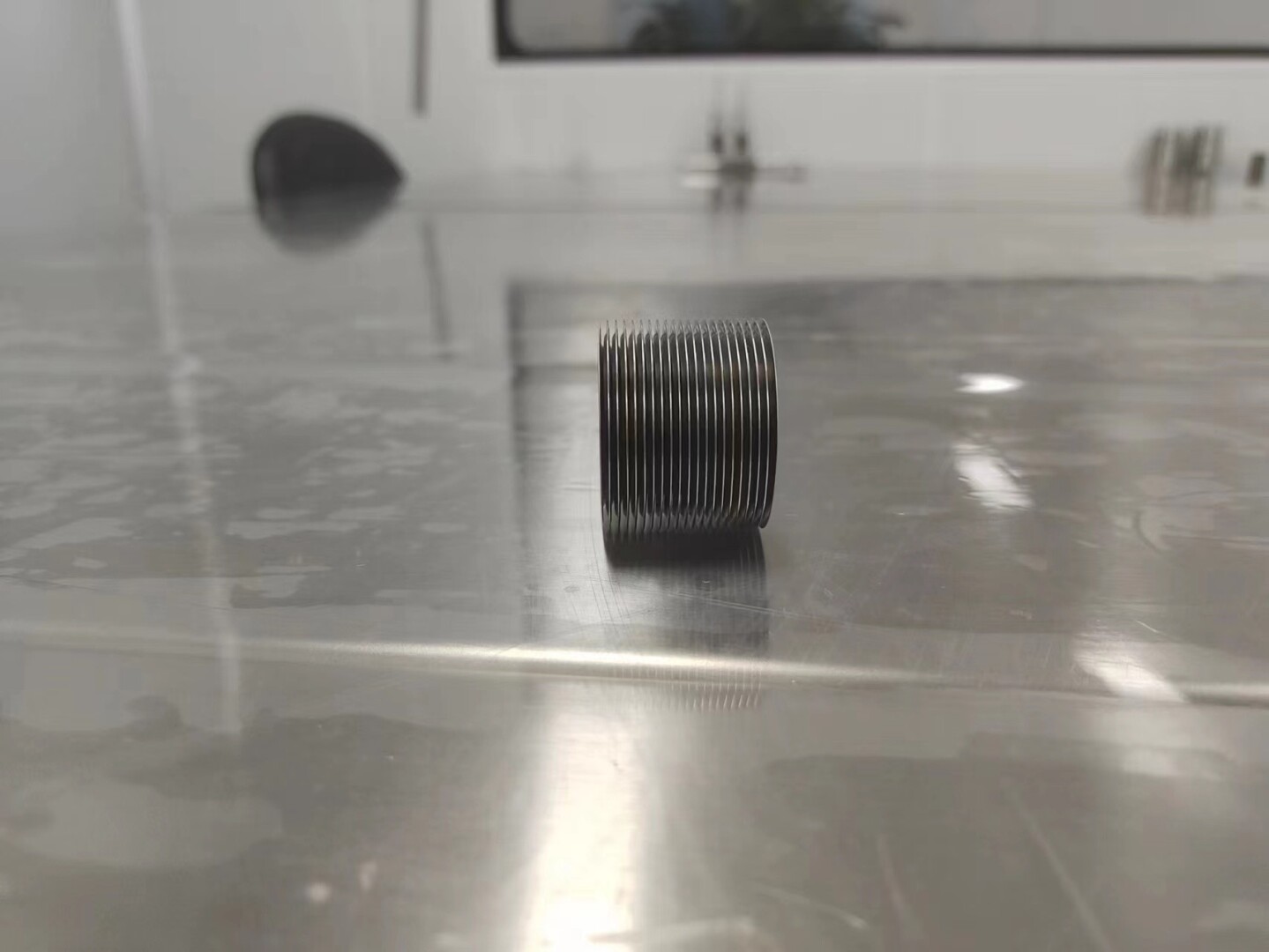
- Edge welded bellows for reactor lift/rotation mechanisms, gas-line flexibility and pump isolation — the bellows technology our own engineering team specializes in.
- Bellows-sealed valves for precursor and purge lines — with the design trade-offs explained in bellows versus diaphragm valve selection.
- High-temperature feedthroughs for heaters — see our high temperature feedthrough guide.
- Gaskets and seals for reactor flanges, specified per our materials guide.
The Alpha Technology Angle
Alpha Technology builds custom edge welded bellows, vacuum feedthroughs and bellows-sealed assemblies for compound-semiconductor equipment — MOCVD reactors, ALD/PECVD tools and sputter systems — helium-leak-tested and cycle-documented. If your GaN program needs hardware that survives hot epitaxy service, contact our engineering team.
FAQ
Why is GaN manufacturing a vacuum business?
GaN epitaxy (MOCVD), gate dielectric deposition (ALD/PECVD), passivation and metallization (PECVD/sputter) and plasma etch all operate in vacuum chambers — the device is built inside vacuum systems from wafer start to metal.
How big is the power GaN market?
Semiconductor Today reports a 35% CAGR toward $3.5 billion by 2031, driven by data centers, EVs and industrial power systems.
What is MOCVD?
Metal-organic chemical vapor deposition grows GaN/AlGaN epitaxial layers on silicon (or SiC/sapphire) at 1,000–1,100°C under reduced pressure — the defining process for GaN power devices.
Which companies are scaling GaN production?
ROHM partnered with AIXTRON on the G10-GaN platform, Samsung ramped an 8-inch GaN line, and Onsemi and GlobalFoundries are developing 650V GaN-on-Si on 200mm wafers.
Building GaN power capacity? Contact Alpha Technology for vacuum hardware rated for hot epitaxy and deposition service.