
In early June 2026, TrendForce reported that Intel and 3DGS planned to invest roughly $3.3 billion in a substrate manufacturing plant in India — the clearest signal yet that glass core substrates are moving from research into industrial production. Industry trackers called 2026 the year glass substrates cross from R&D into pilot and qualification phase, with Intel targeting complete glass substrate solutions in the second half of this decade.
Glass substrates replace organic laminate carriers in advanced packaging, enabling finer lines, larger panels and better dimensional stability for AI accelerators. What gets less attention is how they are made: the manufacturing flow for glass substrates is dominated by vacuum processes.
Why Glass Substrates Matter
Organic substrates warp under heat and cannot hold ultra-fine wiring; silicon interposers work but are expensive and limited in size. Glass core substrates offer a middle path: CTE tunable to match silicon, surface roughness below 1 nm, and the ability to fabricate vias and wiring at panel scale. For AI chips that need thousands of interconnects per square centimeter, glass is the substrate the roadmap is betting on.
The Vacuum Processes Behind a Glass Substrate
1. Through-glass vias (TGV)
Electrical connections pass through the glass core as through-glass vias. The typical flow is: laser ablation or etching to open the via, then PVD seed-layer deposition of Ti/Cu in vacuum, followed by electroplating to fill. The seed layer quality — adhesion, uniformity, step coverage inside the via — sets the via yield, and it is done in vacuum sputter tools with vacuum feedthroughs and bellows-sealed shutters.
2. Metallization and wiring
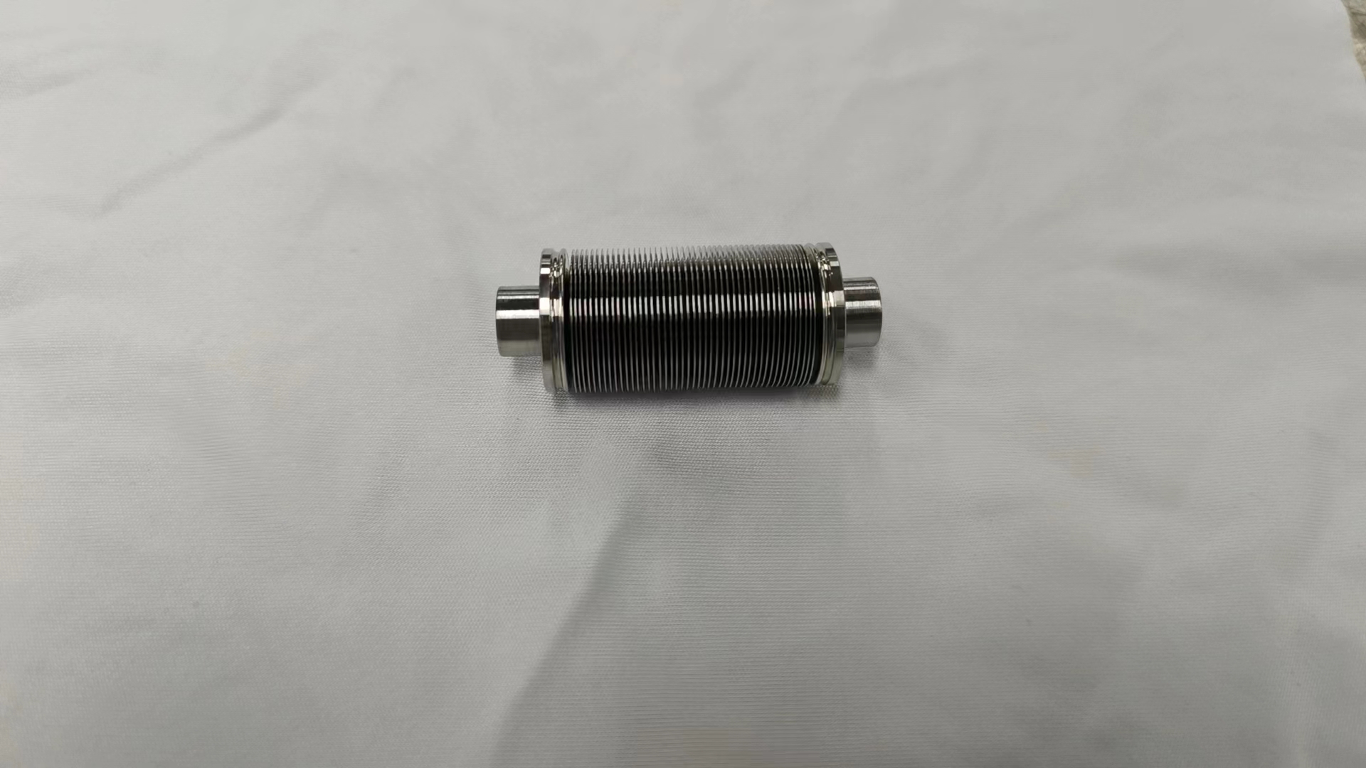
Wiring layers on glass are built by sputtering metal, photolithography and plating. Sputtering is a vacuum process by definition; large glass panels mean large vacuum chambers with long-stroke edge welded bellows for mask handling, shutters and transfer — the same component physics as panel-level packaging lines, applied to panels up to 510×515 mm and beyond.
3. Dielectric deposition and lamination
Insulating layers between wiring planes are deposited by CVD or applied as dry films and laminated under vacuum to avoid trapped air. Vacuum lamination presses use bellows-sealed platens and vacuum feedthroughs for heating and instrumentation; trapped gas is a via-killer.
4. Plasma cleaning and surface treatment
Between every deposition step, panels get plasma treatments — descum, activation, adhesion promotion — all in vacuum chambers. Each treatment chamber is a mini vacuum system with RF feedthroughs, gas panels and leak-tested walls.
The Component Load of a Glass Substrate Fab
- PVD sputter tools: the heart of the line; target shutters, substrate stages and service doors all use edge welded bellows with semiconductor-grade cleanliness.
- Vacuum lamination presses: large bellows and platens rated for panel-size loads; the design guide covers envelope and fatigue engineering.
- Plasma treatment chambers: RF and instrumentation feedthroughs, gas delivery, and 100% leak testing per our leak testing guide.
- Handling and automation: vacuum-compatible robots and load locks keep panels clean between processes; every motion is bellows-sealed.
Cost and Yield Are Vacuum Problems
Glass substrate economics live or die on yield: a single scratch, particle or void in a via becomes a dead interconnect in an expensive AI package. That is why glass fabs adopt semiconductor cleanliness discipline — vacuum processing, cleanroom assembly, serialized component quality. The material choices follow the same logic as our material guide: 316L and specialty alloys that outgas minimally and hold vacuum for years.
What the India Plant Signals
Intel and 3DGS’s $3.3B plant is part of a global buildout: roughly 15 companies now sit in the glass substrate cycle, from materials makers to equipment suppliers, across the US, Asia and Europe. Each plant will consume thousands of vacuum components — sputter targets, bellows, feedthroughs, chambers — creating a new, packaging-driven demand pool that did not exist three years ago. It is the same pattern we analyzed for co-packaged optics and TSMC’s Arizona packaging plant: packaging is becoming a vacuum industry.
Alpha Technology for Glass Substrate and Panel Processing
Alpha Technology supplies custom edge welded bellows, vacuum feedthroughs and formed bellows for PVD, lamination and plasma equipment serving glass substrate and panel-level packaging — panel-scale envelopes, semiconductor-grade cleanliness, leak tested and documented. Contact our engineering team with your chamber and panel dimensions.
FAQ
What is a glass substrate?
A glass core carrier for advanced packaging that replaces organic laminates, offering finer wiring, better dimensional stability and CTE matching to silicon.
Why are glass substrates built with vacuum processes?
Through-glass vias need PVD seed layers, wiring is sputtered, dielectrics are vacuum-laminated, and plasma treatments prepare every surface — the entire flow is vacuum-based.
What is Intel’s glass substrate investment?
Intel and partner 3DGS announced plans for a roughly $3.3 billion substrate plant in India in June 2026, part of a 15-company glass substrate supply chain buildout.
What vacuum components does a glass substrate line need?
Sputter targets, edge welded bellows for shutters and stages, RF and instrumentation feedthroughs, vacuum lamination presses and leak-tested chambers.
Specifying vacuum components for panel processing? Contact Alpha Technology with your panel size, process and cleanliness requirements.