
In July 2026, TSMC reported July revenue up 44.7% year over year as its 2nm process entered mass production, raised 2026 capital expenditure to $60-64 billion (from $56 billion), and announced plans to launch five new fabs during the year, with 2nm capacity growing through 2027. The company also confirmed an additional $100 billion investment in Arizona for 2nm and below.
Every semiconductor reporter has covered the numbers. What’s less discussed is what a 2nm ramp actually requires physically: a 2nm fab is the most vacuum-intensive manufacturing environment ever built. From the EUV scanners at the front of the line to the atomic-layer deposition and etch tools in between, essentially every process step happens inside a sealed chamber held at low pressure, and every chamber is full of vacuum components.
Why 2nm Multiplies the Vacuum Component Count
Moving from 3nm to 2nm (gate-all-around, or GAA, nanosheet transistors) doesn’t just shrink transistors — it adds process steps, and most new steps are vacuum processes:
- Thinner films, more ALD/CVD: nanosheet channels need atomically controlled layers; ALD and CVD tools deposit them in vacuum, with more chambers per tool and more precision per chamber.
- New etch complexity: releasing nanosheets requires highly selective etch steps in plasma reactors — every etch chamber is a vacuum chamber with bellows-sealed stages, RF feedthroughs and gas systems.
- More EUV layers: 2nm uses more EUV passes than any prior node; each EUV scanner is a complete ultra-high-vacuum system, as we covered in High-NA EUV enters production.
- Ion implantation and anneal: source/drain engineering on GAA devices adds implant and anneal steps — vacuum-processed from load lock to cassette.
Where the Vacuum Hardware Lives in a 2nm Fab
1. Load locks and transfer chambers
Every wafer that enters a vacuum tool passes through a load lock — a small chamber that cycles between atmosphere and vacuum, protected by slit valves and transfer arms. Load lock hardware is the highest-cycle-count vacuum hardware in the fab: bellows-sealed gate valves and transfer stages cycle millions of times per year. Our article on edge welded bellows for UHV and semiconductor applications explains why reliability here defines tool availability.
2. Stages, robots and motion systems
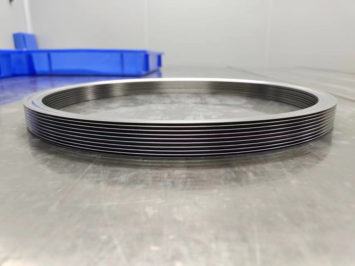
Within each chamber, wafers move on stages and robots whose mechanisms cross the vacuum boundary. Edge welded bellows protect motion mechanisms from process gases while sealing the chamber — the design envelope, stroke and fatigue rules are in our bellows design guide.
3. Feedthroughs for power, RF and sensing
Plasma tools pump kilowatts of RF power into the chamber; sensors, heaters and coolant cross the wall in every tool. Vacuum feedthroughs must hold 1×10⁻⁹ mbar·L/s while carrying high current and surviving thermal cycling — a demanding combination that filters out unqualified suppliers quickly.
4. Materials that match the process
2nm processes run hotter and cleaner. Components in contact with corrosive process gases need 316L, AM350, Inconel or Hastelloy; the right alloy choice is covered in the material guide.
What the Ramp Means for Component Suppliers
With $60-64 billion of annual capex and five new fabs launching in a year, tool OEMs (ASML, Applied Materials, Lam Research, Tokyo Electron and others) are building hundreds of new vacuum tools — each requiring thousands of vacuum components. That demand collides with a supply base where critical parts are frequently single-sourced with 12-20 week lead times. As we noted in our analysis of the $403 billion semiconductor quarter, the companies that qualify a second source now will have capacity when their neighbors don’t.
Alpha Technology for 2nm Tooling
Alpha Technology manufactures custom edge welded bellows, vacuum feedthroughs and formed bellows for semiconductor tool OEMs and fabs — cleanroom assembled, 100% helium leak tested with serialized reports, and available in the alloys 2nm processes demand. We design to your envelope and support full qualification packages. Contact our engineering team with your drawing or envelope.
FAQ
Why does 2nm need more vacuum equipment than older nodes?
GAA transistor architecture adds ALD/CVD, etch and EUV steps, each performed in vacuum chambers; more steps and more EUV layers mean more vacuum tools and more components per tool.
What vacuum level do semiconductor process chambers run at?
Deposition and etch chambers typically run at 10-6 to 10-8 mbar; EUV optical paths and some metrology tools require UHV at 10-8 and below.
How is vacuum hardware qualified for a fab?
With 100% helium leak testing, material certs, cleanroom assembly records and cycle-life validation — the documentation package Alpha Technology ships with every component.
How do I reduce risk in vacuum component supply during the ramp?
Qualify a second source with documented quality, shorter lead times and full traceability before you need it — that is the window Alpha Technology is built to fill.
Qualifying vacuum components for 2nm tooling? Contact Alpha Technology — send your envelope and duty cycle and get a design and real lead time.