
On May 6, 2026, a GlobeNewswire research forecast sized the global molecular beam epitaxy (MBE) system market at $296.9 million for 2026, growing to approximately $588.7 million by 2036 — roughly a 7.1–7.8% CAGR. A broader market analysis published on LinkedIn in July 2026 puts the total MBE market at $1.2 billion in 2024 rising to $2.5 billion by 2033 at 9.2% CAGR, led by compound semiconductors for RF electronics, optoelectronics and quantum computing. The names at the top of the market — Veeco, Riber, SVT Associates, DCA Instruments and Scienta Omicron — all sell one thing in different forms: controlled atomic-layer growth inside ultra-high vacuum.
MBE is the most precise manufacturing process in industry. It grows semiconductor crystals one atomic layer at a time by directing molecular beams at a heated substrate — and it can only do this because the growth chamber holds a vacuum cleaner than any other production environment.
What MBE Demands from Vacuum
Background pressure below 10-10 mbar
An MBE growth chamber operates at a background pressure of 10-10 to 10-11 Torr — several orders of magnitude deeper than a typical process chamber. At these pressures, the time for a single monolayer of residual gas to arrive at the substrate is measured in hours, which is what allows the growing crystal to remain pure while atomic beams arrive at controlled rates.
Beam purity and shutter precision
Effusion cells (Knudsen cells) evaporate gallium, arsenic, indium and dopants at temperatures up to 1,300 °C; mechanical shutters open and close in milliseconds to switch fluxes. The entire assembly — cells, shutters, electrical feedthroughs for heater power, and the rotary drive that spins the substrate — must operate flawlessly in UHV for years between service cycles.
Cryopanel cleanliness
Liquid nitrogen cryopanels surround the growth area and cryopump residual species. Between runs, the chamber is baked and outgassed; the components inside — bellows-sealed transfer arms, viewports, gauges and UHV flanges — must survive hundreds of bake-out cycles at 150–250 °C without developing leaks.
Where the Market Is Growing
- RF and power compound semiconductors — GaN and GaAs for 5G/6G base stations, defense radar and high-efficiency power electronics.
- Photonics and optoelectronics — VCSELs, photodetectors and laser diodes for data centers and lidar.
- Quantum technologies — quantum dot qubits and photonic structures grown with the monolayer precision only MBE provides.
- Emerging memories and sensors — magnetic tunnel junctions and IR detectors grown on MBE lines.
The 9.2% CAGR above the overall semiconductor market reflects exactly where the industry is heading: specialty, high-purity, atomically engineered materials.
How an MBE Run Actually Works
A growth run begins with the chamber at base pressure and the cryopanels cold. Substrate wafers enter through a load lock, are transferred by a bellows-sealed arm, and are heated to the growth temperature while RHEED (reflection high-energy electron diffraction) monitors the surface. Each effusion cell is then heated to its setpoint and its shutter opened in sequence — the molecular beams land on the wafer and crystallize layer by layer, with growth rates measured in tenths of an Angstrom per second. Dopant cells open for fractions of a second to define the electronic profile of the device. The entire choreography happens inside the UHV envelope, which is why reliability of the heater and shutter feedthroughs, the rotary manipulator and the transfer-arm bellows sets the uptime of a production MBE line. A single failing seal can mean a lost epitaxial batch worth thousands of dollars and a day of bake-out to recover.
The Hardware Between the Cells
An MBE system is, mechanically, a study in UHV component engineering:
- Sample manipulators — rotary and linear vacuum feedthroughs carrying substrate heating, rotation and position control into the chamber.
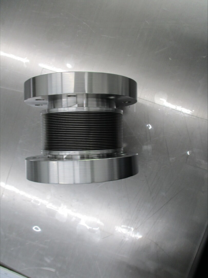
- Bellows-sealed transfer arms — move wafers between load locks and growth position; our edge welded bellows provide the flexing seal with precise stroke control.
- Gate valves — isolate the growth chamber from load locks and analysis chambers without breaking vacuum.
- Viewports and RHEED ports — let operators watch the crystal surface during growth.
- Leak-tight flanges and gaskets — the CF-standard joints that hold 10-11 Torr for years, qualified by helium leak testing at or below 1×10⁻¹⁰ mbar·L/s.
Each of these parts faces a requirement that commercial-grade vacuum hardware cannot meet: consistent performance across hundreds of bake-outs, documented leak rates, and spring and torque characteristics stable enough for sub-micron mechanical repeatability.
The Alpha Technology Angle
Alpha Technology supplies the edge welded bellows, vacuum feedthroughs and sealed assemblies that UHV epitaxy tools rely on — including bellows-sealed motion systems with documented fatigue life and feedthroughs qualified for 250 °C bake-out. Every component ships with helium leak test records and material certifications. Contact our engineering team with your growth chamber specification.
FAQ
Why does MBE require ultra-high vacuum?
At 10-10 to 10-11 Torr, residual gas arrival is measured in hours per monolayer, allowing atomic-layer-pure growth. Higher pressure would contaminate the crystal and ruin the beams.
How big is the MBE market?
The MBE system market is about $296.9 million in 2026 growing to $588.7 million by 2036; the broader MBE market is projected from $1.2 billion (2024) to $2.5 billion (2033) at 9.2% CAGR.
What vacuum components are inside an MBE chamber?
Effusion cell feedthroughs, rotary and linear sample manipulators, bellows-sealed transfer arms, gate valves, cryopanels, viewports and CF flanges — all UHV-qualified and bake-out compatible.
Which industries use MBE?
Compound semiconductor RF, photonics, quantum dots and quantum computing, magnetic sensors and infrared detectors — all growing faster than mainstream silicon.
Qualifying UHV hardware for an epitaxy or deposition tool? Contact Alpha Technology for leak-tested, documented components.